Hardware Design Files
This folder is reserved for KiCad hardware design files for the DCC Locomotive Decoder.
Planned Contents
- Schematic: Complete circuit schematic (
.kicad_sch) - PCB Layout: Printed circuit board design (
.kicad_pcb) - Bill of Materials: Component list (BOM.csv)
- Gerber Files: Manufacturing files
- 3D Models: Component models
- Assembly Drawings: Assembly instructions
Current Status
🚧 Under Development
Hardware design files will be added in future releases.
Design Goals
- Compact form factor suitable for HO/N scale locomotives
- Single or dual-sided PCB (TBD)
- Through-hole or SMD components (TBD)
- Easy assembly and testing
- Robust protection circuits
- Proper EMI/EMC considerations
Sections
The PCB will include the following sections:
-
Power Supply
- Track power input with TVS protection
- Schottky diode bridge rectifier (4x SS54: 5A, 40V)
- Bulk filtering capacitors (470µF-1000µF electrolytic)
- 3.3V LDO regulator for ESP32-H2 logic
- Separate motor power feed to TB67H450FNG VM pin
- Ceramic bypass capacitors (0.1µF near ICs)
-
DCC Input Stage
- Optocoupler isolation
- Signal conditioning
- Protection diodes
-
Motor Driver
- TB67H450FNG H-bridge
- Current sense circuit (0.1Ω shunt resistor)
- Bootstrap capacitors (if needed for gate drive)
- Flyback diodes (usually internal to TB67H450FNG)
- Bulk motor power capacitor (100µF near VM pin)
-
Microcontroller
- ESP32-H2 module or bare chip
- Programming header
- Reset and boot buttons
-
LED Output
- WS2812 connector
- Level shifter (if needed)
- Power filtering
-
RailCom
- RailCom transmitter circuit
- Cutout detection
- Track coupling circuit
-
Accessory Outputs
- 2x N-FET drivers
- Screw terminals or connectors
- Protection circuits
-
Configuration
- Configuration button
- Status LED
- Optional programming port
Component Selection
Key Components
- Bridge Rectifier: 4x SS54 Schottky diodes (5A, 40V, SMA/DO-214AC) or SS56 (5A, 60V)
- Lower forward drop (~0.5V per diode, 1V total vs 2V for standard bridge)
- Better efficiency = less heat
- Fast switching for DCC frequency
- Arrange in standard bridge configuration
- Microcontroller: ESP32-H2 (RISC-V, Zigbee/Thread)
- Motor Driver: Toshiba TB67H450FNG (dual H-bridge, 3.5A)
- Optocoupler: 6N137 (fast) or PC817 (general purpose)
- N-FETs: AO3400A (SOT-23, 4A, 44mΩ RDS(on) @ 2.5V)
- For accessory outputs (max 350mA each)
- Logic-level compatible with 3.3V GPIO
- Low cost (~$0.05-0.10)
- Voltage Regulator: AMS1117-3.3 (800mA) or HT7333 (LDO, low dropout)
- Current Sense Resistor: 0.1Ω, 1W metal film or wire-wound
- LEDs: WS2812B or compatible addressable RGB LEDs
Connectors
- Motor: 2-pin screw terminal or JST-XH
- Track Input: 2-pin screw terminal
- LED Strip: 3-pin JST connector
- Accessories: 2x 2-pin screw terminals
- Programming: 6-pin header (GND, 3V3, TX, RX, IO0, EN)
Design Considerations
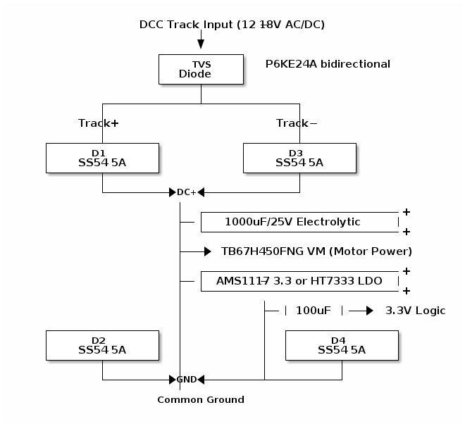
Power Supply Schematic
                DCC Track Input (12-18V AC/DC)
                          |
                          v
                    +-----+-----+
                    |    TVS    | P6KE24A bidirectional
                    |  Diode    |
                    +-----+-----+
                          |
            +-------------+-------------+
            |                           |
         Track+                      Track-
            |                           |
    +-------+-------+           +-------+-------+
    |      D1       |           |      D3       |
    |    SS54 5A    |           |    SS54 5A    |
    +-------+-------+           +-------+-------+
            |                           |
            +--------->DC+<-------------+
                       |
                       |  +----------------------------+
                       +--| 1000uF/25V Electrolytic   |
                       |  +----------------------------+
                       |
                       +---> TB67H450FNG VM (Motor Power)
                       |
                       |  +----------------------------+
                       +--| AMS1117-3.3 or HT7333 LDO |
                       |  +----------------------------+
                       |           |
                       |           +--| 100uF |---> 3.3V Logic
                       |           |
    +-------+-------+  |           |  +-------+-------+
    |      D2       |  |           |  |      D4       |
    |    SS54 5A    |  |           |  |    SS54 5A    |
    +-------+-------+  |           |  +-------+-------+
            |          |           |          |
            +--------->GND<--------+----------+
                       |
                    Common Ground
Bridge Configuration:
- Track inputs: Connect to DCC rails (polarity-independent)
- DC+ rail: 10-16V after rectification
- Forward drop: ~1V total (0.5V per diode pair)
- SS54 Schottky: 5A continuous, 40V rating
- Handles motor (1-3A) + logic (~200mA) simultaneously
Component Values:
- Bridge: 4x SS54 (SMA package)
- Bulk cap: 1000µF/25V electrolytic
- LDO input cap: 10µF ceramic
- LDO output cap: 100µF electrolytic + 0.1µF ceramic
- TVS: P6KE24A or 1.5KE24CA
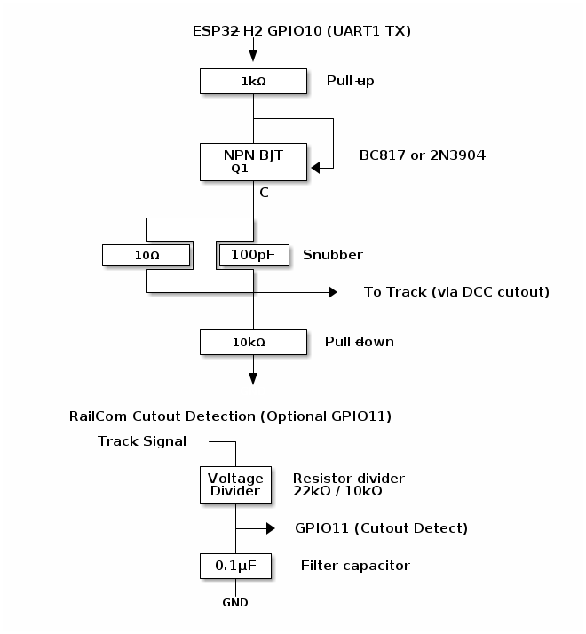
RailCom Transmitter Schematic
                   ESP32-H2 GPIO10 (UART1 TX)
                          |
                          v
                    +-----+-----+
                    |    1kΩ    | Pull-up
                    +-----+-----+
                          |
                          +--------+
                          |        |
                    +-----+-----+  |
                    |  NPN BJT  |  |  BC817 or 2N3904
                    |   Q1      |<-+
                    +-----+-----+
                          |C
                          |
              +-----------+
              |           |
         +----+----+  +---+---+
         |   10Ω   |  | 100pF | Snubber
         +----+----+  +---+---+
              |           |
              +-----------+--------> To Track (via DCC cutout)
                          |
                          |
                    +-----+-----+
                    |   10kΩ    | Pull-down
                    +-----+-----+
                          |
                          v
                         GND

   RailCom Cutout Detection (Optional GPIO11)

        Track Signal ---+
                        |
                    +---+---+
                    |Voltage|  Resistor divider
                    |Divider|  22kΩ / 10kΩ
                    +---+---+
                        |
                        +---> GPIO11 (Cutout Detect)
                        |
                    +---+---+
                    | 0.1µF | Filter capacitor
                    +---+---+
                        |
                       GND
RailCom Operation:
- Cutout Detection: DCC command station creates ~450µs cutout window
- Channel Timing:
- Channel 1: 26-177µs (address broadcast)
- Channel 2: 193-454µs (status data)
- Transmit: UART TX at 250kbaud during cutout
- Encoding: 4-to-8 bit encoding per RailCom spec
Components:
- Q1: BC817 NPN (SOT-23) or 2N3904
- R1: 1kΩ base resistor
- R2: 10Ω series resistor (current limit)
- R3: 10kΩ pull-down
- C1: 100pF snubber capacitor
- Cutout divider: 22kΩ + 10kΩ (scales track voltage to 3.3V)
Important Notes:
- RailCom transmits ONLY during DCC cutout window
- Requires command station with RailCom support
- Cutout detection is optional (can use timing from last DCC packet)
- Q1 must switch fast enough for 250kbaud (BC817: fT=100MHz)
Thermal Management
- Adequate copper pour for motor driver heat dissipation
- Thermal vias under motor driver IC
- Consider adding heatsink mounting holes
- Keep power traces wide (minimum 2mm for motor power)
- Bridge diodes: Place on copper pour for heat spreading
Layout Guidelines
- Keep DCC input traces short and isolated
- Star ground topology for power
- Separate analog and digital grounds near ADC
- Shield sensitive signals (DCC input, current sense)
- Keep high-speed traces short (WS2812 data <10cm)
- Proper decoupling capacitors near ICs (0.1µF within 5mm)
- Wide traces for rectifier output (2-3mm minimum)
Protection
-
TVS diode on track input (P6KE24A bidirectional)
-
Schottky diodes provide inherent fast response
-
Reverse polarity protection on track input
-
TVS diodes on all external connections
-
Overcurrent protection on motor output
-
ESD protection on user-accessible pins
Testing
- Test points for key signals (DC+, 3.3V, DCC signal, motor outputs)
- LED indicators for power (3.3V rail), DCC signal presence, status
- Easy access to programming pins
- Measure bridge rectifier forward drop (should be ~1V under load)
- Current sense test point for motor current monitoring
Future Enhancements
- Dual motor driver option
- Sound module integration (I2S DAC)
- Additional function outputs
- Servo outputs (2-4 channels)
- SUSI interface
- Optional Bluetooth antenna
Contributing
If you'd like to contribute to the hardware design:
- Use KiCad 7.0 or newer
- Follow IPC design standards
- Include clear documentation
- Provide design rationale for key decisions
- Test thoroughly before sharing
References
License
Hardware designs will be released under CERN Open Hardware License v2 - Permissive (CERN-OHL-P).
Status: Planned for future release Last Updated: 2026-01-15

